- 您现在的位置:买卖IC网 > Sheet目录3818 > PIC18F4620-I/ML (Microchip Technology)IC MCU FLASH 32KX16 44QFN
PIC18C601/801
DS39541A-page 292
Advance Information
2001 Microchip Technology Inc.
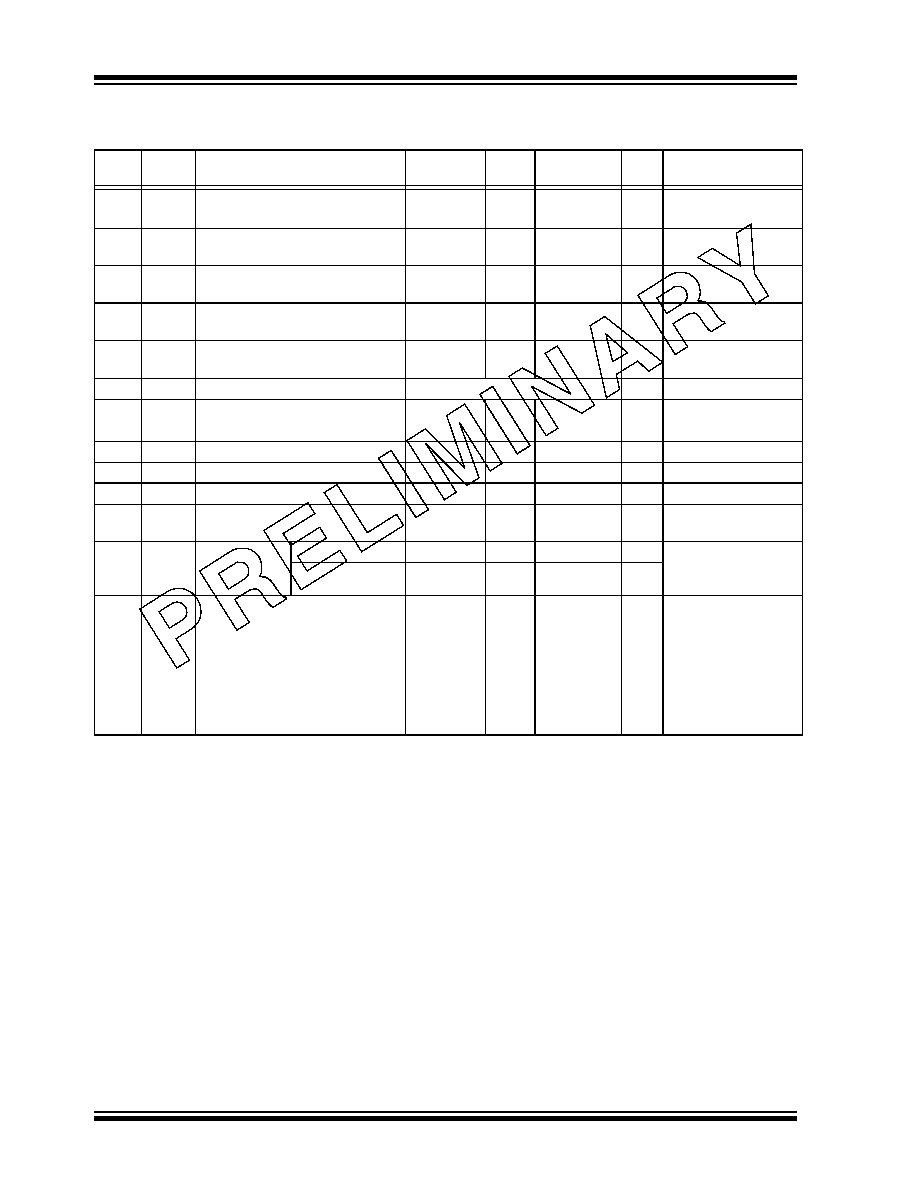
TABLE 22-22: A/D CONVERTER CHARACTERISTICS: PIC18C601/801 (INDUSTRIAL, EXTENDED)
PIC18LC601/801 (INDUSTRIAL)
Param
No.
Symbol
Characteristic
Min
Typ
Max
Units
Conditions
A01
NR
Resolution
—
10
TBD
bit
VREF = VDD
≥ 3.0V
VREF = VDD
< 3.0V
A03
EIL
Integral linearity error
—
<±1
TBD
LSb
VREF = VDD
≥ 3.0V
VREF = VDD
< 3.0V
A04
EDL
Differential linearity error
—
<±1
TBD
LSb
VREF = VDD
≥ 3.0V
VREF = VDD
< 3.0V
A05
EFS
Full scale error
—
<±1
TBD
LSb
VREF = VDD
≥ 3.0V
VREF = VDD
< 3.0V
A06
EOFF
Offset error
—
<±1
TBD
LSb
VREF = VDD
≥ 3.0V
VREF = VDD
< 3.0V
A10
—
Monotonicity
guaranteed(3)
—
VSS
≤ VAIN ≤ VREF
A20
VREF
Reference voltage
(VREFH - VREFL)
0
——
V
A20A
3
——
V
For 10-bit resolution
A21
VREFH
Reference voltage High
AVSS
—
AVDD + 0.3 V
V
A22
VREFL
Reference voltage Low
AVSS - 0.3 V
—
AVDD
V
A25
VAIN
Analog input voltage
AVSS - 0.3 V
—
VREF + 0.3 V
V
A30
ZAIN
Recommended impedance of
analog voltage source
——
10.0
k
A40
IAD
A/D conversion
current (VDD)
PIC18C601/801
—
180
—
A Average current
consumption when
A/D is on(1)
PIC18LC601/801
—
90
—
A
A50
IREF
VREF input current(2)
10
—
1000
10
A
During VAIN acquisition.
Based on differential of
VHOLD to VAIN. To
charge CHOLD, see
During A/D conversion
cycle.
Note 1: When A/D is off, it will not consume any current other than minor leakage current. The power-down current
spec includes any such leakage from the A/D module.
VREF current is from RA2/AN2/VREF- and RA3/AN3/VREF+ pins or AVDD and AVSS pins, whichever is
selected as reference input.
2: Vss
≤ VAIN ≤ VREF
3: The A/D conversion result either increases or remains constant as the analog input increases.
发布紧急采购,3分钟左右您将得到回复。
相关PDF资料
PIC24HJ256GP210-I/PT
IC PIC MCU FLASH 128KX16 100TQFP
PIC24HJ128GP310A-I/PF
IC PIC MCU FLASH 128KB 100-TQFP
DSPIC33FJ128GP310-I/PF
IC DSPIC MCU/DSP 128K 100TQFP
PIC16C66-20I/SO
IC MCU OTP 8KX14 PWM 28SOIC
DSPIC33FJ128MC510-I/PT
IC DSPIC MCU/DSP 128K 100TQFP
PIC16C66-20I/SP
IC MCU OTP 8KX14 PWM 28DIP
PIC18LF2620-I/SP
IC MCU FLASH 32KX16 28SDIP
PIC16F877-04I/P
IC MCU FLASH 8KX14 EE 40DIP
相关代理商/技术参数
PIC18F4620-I/P
功能描述:8位微控制器 -MCU 64KB 3968 RAM 36 I/O RoHS:否 制造商:Silicon Labs 核心:8051 处理器系列:C8051F39x 数据总线宽度:8 bit 最大时钟频率:50 MHz 程序存储器大小:16 KB 数据 RAM 大小:1 KB 片上 ADC:Yes 工作电源电压:1.8 V to 3.6 V 工作温度范围:- 40 C to + 105 C 封装 / 箱体:QFN-20 安装风格:SMD/SMT
PIC18F4620-I/P
制造商:Microchip Technology Inc 功能描述:IC 8BIT FLASH MCU 18F4620 DIP40
PIC18F4620-I/PT
功能描述:8位微控制器 -MCU 64KB 3968 RAM 36 I/O RoHS:否 制造商:Silicon Labs 核心:8051 处理器系列:C8051F39x 数据总线宽度:8 bit 最大时钟频率:50 MHz 程序存储器大小:16 KB 数据 RAM 大小:1 KB 片上 ADC:Yes 工作电源电压:1.8 V to 3.6 V 工作温度范围:- 40 C to + 105 C 封装 / 箱体:QFN-20 安装风格:SMD/SMT
PIC18F4620-I/PT
制造商:Microchip Technology Inc 功能描述:IC 8BIT FLASH MCU 18F4620 TQFP44
PIC18F4620T-I/ML
功能描述:8位微控制器 -MCU 64KB 3968 RAM 36 I/O RoHS:否 制造商:Silicon Labs 核心:8051 处理器系列:C8051F39x 数据总线宽度:8 bit 最大时钟频率:50 MHz 程序存储器大小:16 KB 数据 RAM 大小:1 KB 片上 ADC:Yes 工作电源电压:1.8 V to 3.6 V 工作温度范围:- 40 C to + 105 C 封装 / 箱体:QFN-20 安装风格:SMD/SMT
PIC18F4620T-I/PT
功能描述:8位微控制器 -MCU 64KB 3968 RAM 36 I/O RoHS:否 制造商:Silicon Labs 核心:8051 处理器系列:C8051F39x 数据总线宽度:8 bit 最大时钟频率:50 MHz 程序存储器大小:16 KB 数据 RAM 大小:1 KB 片上 ADC:Yes 工作电源电压:1.8 V to 3.6 V 工作温度范围:- 40 C to + 105 C 封装 / 箱体:QFN-20 安装风格:SMD/SMT
PIC18F4680-E/ML
功能描述:8位微控制器 -MCU 64KB 3328 RAM w/ECAN RoHS:否 制造商:Silicon Labs 核心:8051 处理器系列:C8051F39x 数据总线宽度:8 bit 最大时钟频率:50 MHz 程序存储器大小:16 KB 数据 RAM 大小:1 KB 片上 ADC:Yes 工作电源电压:1.8 V to 3.6 V 工作温度范围:- 40 C to + 105 C 封装 / 箱体:QFN-20 安装风格:SMD/SMT
PIC18F4680-E/P
功能描述:8位微控制器 -MCU 64KB 3328 RAM w/ECAN RoHS:否 制造商:Silicon Labs 核心:8051 处理器系列:C8051F39x 数据总线宽度:8 bit 最大时钟频率:50 MHz 程序存储器大小:16 KB 数据 RAM 大小:1 KB 片上 ADC:Yes 工作电源电压:1.8 V to 3.6 V 工作温度范围:- 40 C to + 105 C 封装 / 箱体:QFN-20 安装风格:SMD/SMT